Vacuum Coating–The Existing Crystal Coating Method
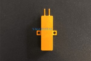
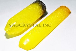
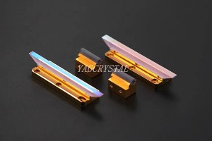
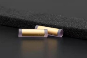
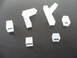
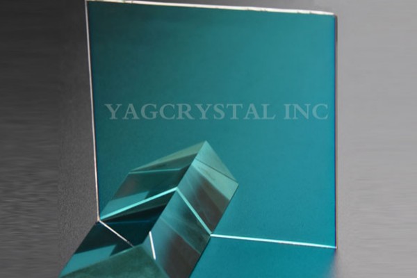
Product Description
The existing crystal coating method includes: dividing a large crystal into equal-area medium crystals, then stacking a plurality of medium crystals, and bonding two adjacent medium crystals with glue; Divide into multiple groups of equal-area stacked small crystals again; take a stack of small crystals, and polish the peripheral sides of the multiple small crystals to obtain small crystals with a circular cross section; Separation; taking one of the small crystals, and applying protective glue on the circumferential side walls of the small crystals; coating the front and/or reverse sides of the small crystals; removing the protective glue on the circumferential sides of the small crystals to obtain the final product.
The existing crystal coating processing method needs to protect the circumferential side wall of the wafer. For small wafers, it is easy to pollute the upper and lower surfaces when applying glue, and the operation is not easy. When the front and back of the crystal are coated After the end, the protective glue needs to be washed off, and the operation steps are cumbersome.
Methods
The coating method of the crystal comprises:
● Along the preset cutting contour, using a laser to incident from the upper surface of the substrate to perform modified cutting inside the substrate to obtain the first intermediate product;
● Coating the upper surface and/or the lower surface of the first intermediate product to obtain a second intermediate product;
● Along the preset cutting contour, the upper surface of the second intermediate product is scribed and cut with a laser, and the wafer is split, so as to separate the target product from the leftover material.